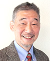
Keynote Speaker

-
Session 13
Advanced and Affordable EUV Lithography with Deep-Dive Mitigation of ML Defects
- Yoshihiro Tezuka (Intel K.K., Japan)
Biography
Received BS, MS, and Ph.D. degrees, all in Physics from the University of Tokyo in 1986, 1988, and 1991, respectively. Worked in Kawasaki Steel LSI Research Center and Tokyo Electron Ltd totally for 7 years, then joined intel in 1997 as a starting member of collaboration project with DNP for advanced mask development. After deployment to Intel Mask Operations (IMO) Santa Clara, assigned to Japan’s Consortium MIRAI in 2001 representing intel, and initiated Actinic Blank Inspection project from scratch. Since then, living in Tsukuba-city even after returning to IMO’s reporting line in 2007 by remotely joining IMO technology development team in many projects such as e-beam writer enhancements, multibeam writer development, and actinic patterned mask inspection tool development and integration.